We help the world since 2012

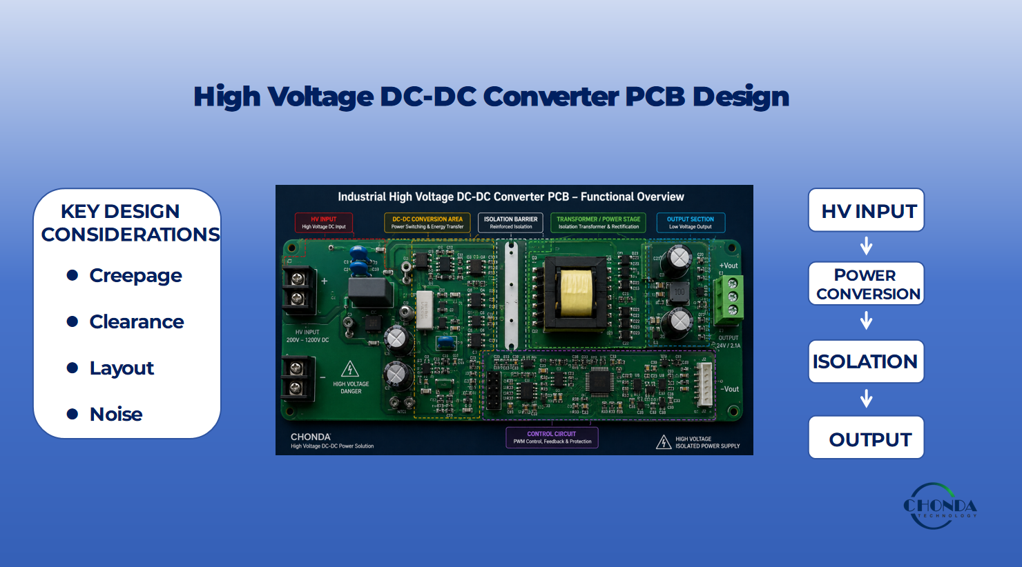
High Voltage DC-DC Converter PCB Design Considerations
Designing a PCB for a high voltage DC-DC converter requires more than simply connecting the input, output, and control circuits.
At higher DC input voltages, PCB layout directly affects electrical safety, insulation reliability, electromagnetic noise, signal integrity, and long-term system stability.
For applications such as PV string monitoring, solar combiner boxes, industrial automation, robotics, and other embedded power systems, several PCB layout factors should be considered from the beginning of the design process.
The most important considerations include creepage, clearance, high-voltage routing, switching noise, and grounding.
1. Creepage Distance
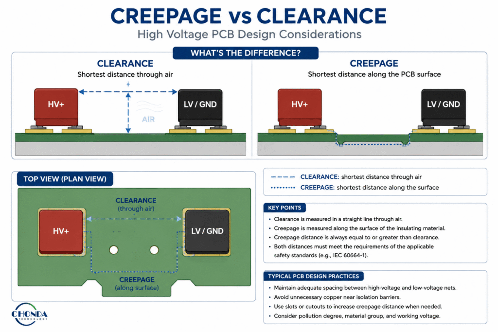
Creepage distance is the shortest distance between two conductive parts measured along the surface of an insulating material, such as the PCB.
In a high-voltage DC-DC converter, sufficient creepage distance is important for maintaining insulation reliability and reducing the risk of surface tracking or insulation breakdown.
The required creepage distance depends on factors such as:
- Working voltage
- Insulation type
- Pollution degree
- PCB material
- Material group
- Altitude
- Applicable safety standard
For high-voltage applications, designers should determine the required creepage distance according to the applicable insulation-coordination requirements rather than relying on a generic PCB spacing rule. IEC 60664-1 provides requirements and methods related to creepage, clearance, and solid insulation for equipment within its scope.
Practical PCB considerations
When routing a high-voltage isolation barrier:
- Keep high-voltage conductors sufficiently separated.
- Avoid unnecessary copper near the isolation boundary.
- Consider slots or cutouts when additional creepage distance is required.
- Avoid sharp conductive features close to the isolation barrier.
- Check the actual PCB geometry rather than measuring only the schematic.
A PCB may satisfy a basic electrical connection requirement while still failing to provide adequate physical insulation.
2. Clearance Distance
Clearance is the shortest distance through air between two conductive parts.
Unlike creepage, clearance does not follow the PCB surface.
For example, the distance between a high-voltage trace and an adjacent low-voltage trace across an air gap is a clearance distance.
This becomes particularly important when a DC-DC converter operates with a high input voltage and requires isolation between the input and output sides.
A good PCB design should therefore clearly define:
High-voltage side → isolation barrier → low-voltage side
and avoid allowing unnecessary copper, vias, test points, or other conductive structures to cross the isolation boundary.
Clearance requirements are determined by the applicable insulation and safety requirements, so the designer should not simply assume that a particular number of millimeters is universally sufficient.
3. High-Voltage PCB Layout
High-voltage PCB layout should be planned before routing begins.
A useful approach is to divide the PCB into functional areas:
High-voltage input section
This section may include:
- HV input terminals
- Input protection
- Filtering
- Rectification or switching components
- High-voltage capacitors
Power conversion section
This is where the main switching energy is processed.
Keep high-current and high-frequency loops as small as practical.
Low-voltage output section
This section may contain:
- Output filtering
- Feedback circuits
- Control electronics
- Communication interfaces
- Sensors
Control and sensitive signal section
Keep sensitive feedback and measurement circuits away from high dv/dt switching nodes whenever possible.
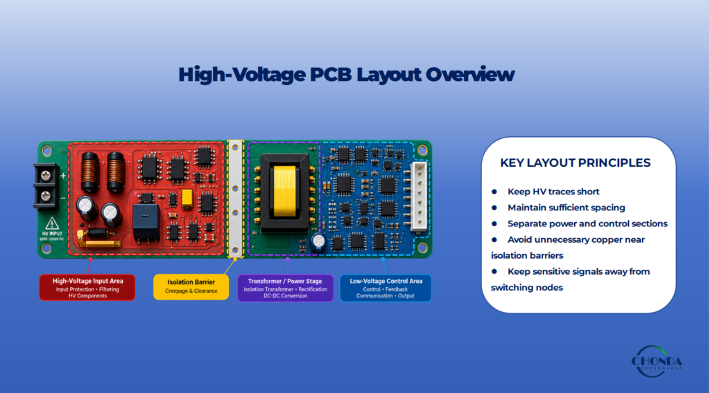
The physical arrangement should follow the electrical flow of the power converter rather than simply filling available PCB space.
Analog Devices similarly recommends identifying power paths and reducing current-loop areas as part of power PCB layout planning.
4. Keep High dv/dt Nodes Short
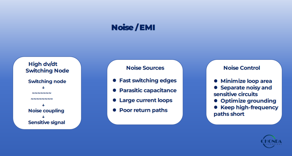
One of the most important considerations in a switching converter is the high dv/dt switching node.
A rapidly changing voltage can couple unwanted energy into nearby traces, planes, and components through parasitic capacitance.
Therefore:
- Keep high dv/dt copper areas as small as practical.
- Avoid routing sensitive signal traces close to switching nodes.
- Do not run feedback traces underneath noisy switching areas unless the design specifically provides appropriate shielding.
- Keep switching loops compact.
- Place associated components close together.
This is particularly important when the converter is installed in a system containing sensitive measurement, communication, or monitoring electronics.
A well-designed PCB reduces noise at its source instead of trying to remove the noise after it has already spread through the system.
5. Noise and EMI Considerations
High-voltage DC-DC converters are switching power systems, so electromagnetic noise is an important design consideration.
Noise can be coupled through:
- Conductive paths
- Parasitic capacitance
- Ground impedance
- Magnetic coupling
- Long PCB traces
- Large switching loops
Common sources include high-frequency switching nodes, transformer or inductor current loops, fast gate-drive signals, and poorly controlled return paths.
How can PCB layout reduce noise?
Several practical approaches can help:
Minimize current-loop area
Shorter and more compact switching loops generally reduce parasitic inductance and unwanted radiation.
Separate noisy and sensitive circuits
Keep high-frequency switching nodes away from:
- Feedback circuits
- Analog measurement circuits
- Communication interfaces
- Sensor signals
Keep sensitive traces short
Long traces can behave like antennas and increase the opportunity for noise coupling.
Use appropriate decoupling
Place bypass and decoupling capacitors close to the relevant power pins or switching devices to provide a low-impedance high-frequency current path.
6. Grounding Strategy
Grounding is another critical part of DC-DC converter PCB design.
However, there is no universal rule that every PCB should simply “split the ground plane.”
The correct grounding strategy depends on the converter topology, isolation architecture, switching currents, control circuitry, and system requirements.
For example, an isolated high-voltage DC-DC converter may have:
- Primary-side ground
- Secondary-side ground
- Power ground
- Control or signal ground
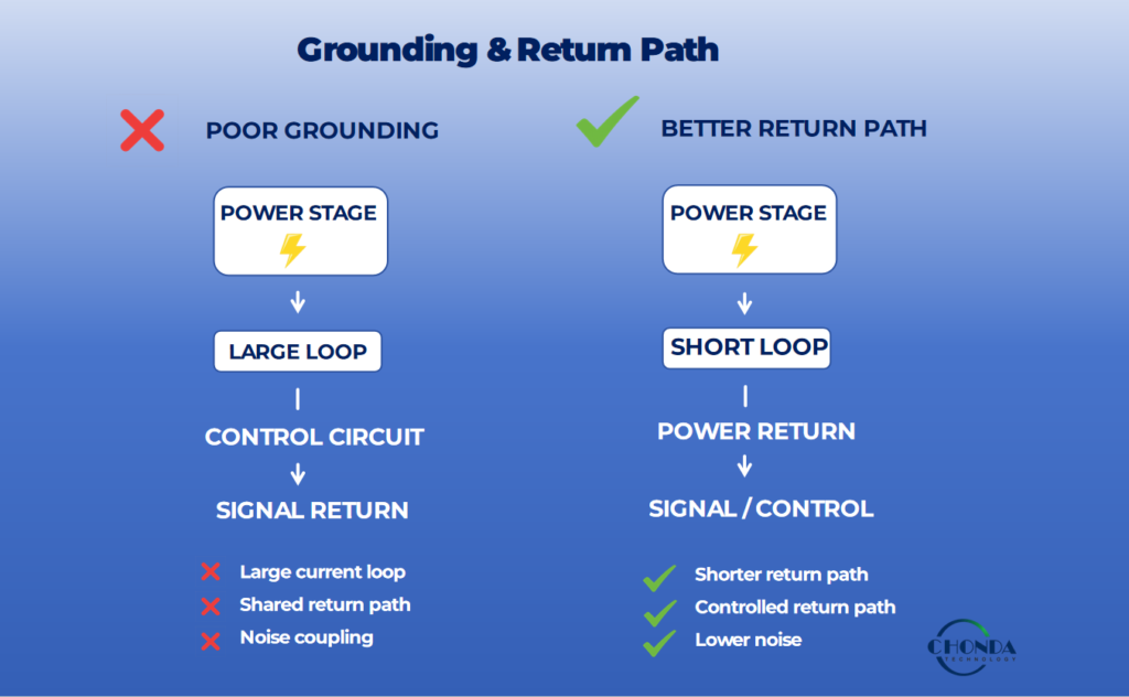
The return path of each important current should be understood before deciding how the ground planes are arranged.
A low-impedance ground plane can provide a controlled return path and reduce unwanted voltage differences caused by parasitic impedance.
Avoid uncontrolled return paths
One common PCB problem occurs when a sensitive signal shares part of the return path with a high-current switching circuit.
The switching current can create voltage fluctuations across the shared impedance.
The result may include:
- Feedback instability
- Measurement errors
- Communication interference
- Increased EMI
- Unexpected system noise
Therefore, designers should always ask:
Where does the current flow, and where does its return current flow?
Understanding the complete current loop is often more useful than simply following a generic grounding rule.
7. Maintain the Isolation Barrier
For an isolated high-voltage DC-DC converter, the isolation barrier should be treated as a physical design boundary.
Do not allow the following to unintentionally compromise the barrier:
- Copper pours
- Traces
- Vias
- Test points
- Mounting hardware
- Heatsinks
- Connectors
- Contamination or conductive debris
The PCB should maintain the required creepage and clearance throughout the entire isolation path.
In some designs, PCB slots or cutouts can be used to increase the surface distance available between conductive regions.
For high-voltage and high-frequency systems, isolation-barrier geometry can also affect parasitic capacitance and EMI behavior.
8. PCB Layout Should Be Considered Early
PCB layout should not be treated as the final step after the circuit has already been designed.
For a high-voltage DC-DC converter, layout decisions can affect:
- Insulation performance
- Switching losses
- Thermal performance
- EMI
- Output regulation
- Feedback stability
- Reliability
- Manufacturing cost
A better design process is to consider the PCB architecture during the early power-supply design stage.
Before routing, engineers should identify:
- High-voltage regions
- Isolation barriers
- Main power loops
- High dv/dt nodes
- Sensitive signal paths
- Ground-return paths
- Thermal hotspots
- Required creepage and clearance
This makes it much easier to develop a reliable layout than trying to solve these issues after routing is complete.
9. High Voltage Does Not Mean “Just Increase the Spacing”
A common misconception is that high-voltage PCB design simply means increasing the distance between traces.
In reality, a reliable high-voltage DC-DC converter requires a combination of:
Electrical insulation + PCB geometry + current-loop control + noise management + grounding + thermal design
For example, increasing the distance between two traces may improve isolation, but it does not automatically solve switching noise caused by a large current loop.
Similarly, a large ground plane may provide a low-impedance return path, but it must not unintentionally cross an isolation barrier.
The PCB must therefore be considered as an integrated electrical and physical system.
10. Practical High-Voltage PCB Checklist
Before releasing a high-voltage DC-DC converter PCB for manufacturing, engineers can review the following checklist:
Insulation
☐ Required creepage distance has been verified.
☐ Required clearance distance has been verified.
☐ Isolation barriers are clearly defined.
☐ No unnecessary copper crosses the isolation barrier.
☐ Vias and test points maintain the required spacing.
High-Voltage Layout
☐ High-voltage traces are routed intentionally.
☐ High dv/dt nodes are minimized.
☐ High-current loops are kept compact.
☐ Sensitive circuits are separated from noisy power stages.
Noise
☐ Switching loops are minimized.
☐ Feedback traces are routed away from noisy nodes.
☐ Decoupling components are located close to their relevant devices.
☐ Potential EMI coupling paths have been considered.
Ground
☐ Power-current return paths are clearly understood.
☐ Sensitive signals do not share inappropriate high-current return paths.
☐ Ground planes are used according to the converter topology.
☐ Isolation between primary and secondary grounds is maintained where required.
Conclusion
PCB design is one of the most important factors in the reliability of a high-voltage DC-DC converter.
Creepage and clearance provide the physical foundation for electrical insulation, while high-voltage routing, switching-loop control, noise management, and grounding determine how reliably the converter performs in a real system.
For applications such as PV string monitoring, solar combiner boxes, industrial automation, robotics, and embedded power systems, these considerations should be addressed from the earliest stage of the design.
A well-designed converter is not only electrically functional. It must also provide the required isolation, reliability, EMC performance, and long-term stability within the complete system.
For engineers evaluating a high-voltage DC-DC module, PCB requirements should therefore be considered together with the module’s input voltage range, isolation voltage, output requirements, thermal conditions, and application environment.
CHONDA provides high-voltage DC-DC power modules for PV monitoring and industrial applications, with flexible specifications and custom design support for application-specific requirements.
Related Articles
How to Select a DC-DC Converter for PV Monitoring Applications
Learn how input voltage range, output requirements, isolation, and power ratings affect DC-DC converter selection for PV string monitoring systems.
PV String Monitoring vs. Inverter Monitoring: What’s the Difference?
Understand the key differences between PV string monitoring and inverter-level monitoring, and why isolated power supplies are important in monitoring applications.
Why PV Monitoring Systems Need Isolated Power Supplies
Explore how isolated DC-DC power modules can provide reliable auxiliary power for high-voltage PV monitoring and control systems.
High Voltage DC-DC Converter for Industrial Automation | CHONDA
Explore how high-voltage DC-DC converters can support reliable power conversion in industrial automation and other demanding applications.