We help the world since 2012

EMC of AC-DC Converters: Common Noise Sources and Design Considerations
Electromagnetic compatibility (EMC) is an important design consideration for AC-DC converters used in industrial power systems.
An AC-DC converter must not only deliver the required electrical power. It must also operate without creating unacceptable electromagnetic disturbances for the equipment itself or for other equipment connected to the same electrical environment.
This becomes particularly important when the converter contains high-frequency switching devices, rectification stages, PFC circuits, transformers, inductors, and large energy-storage components.
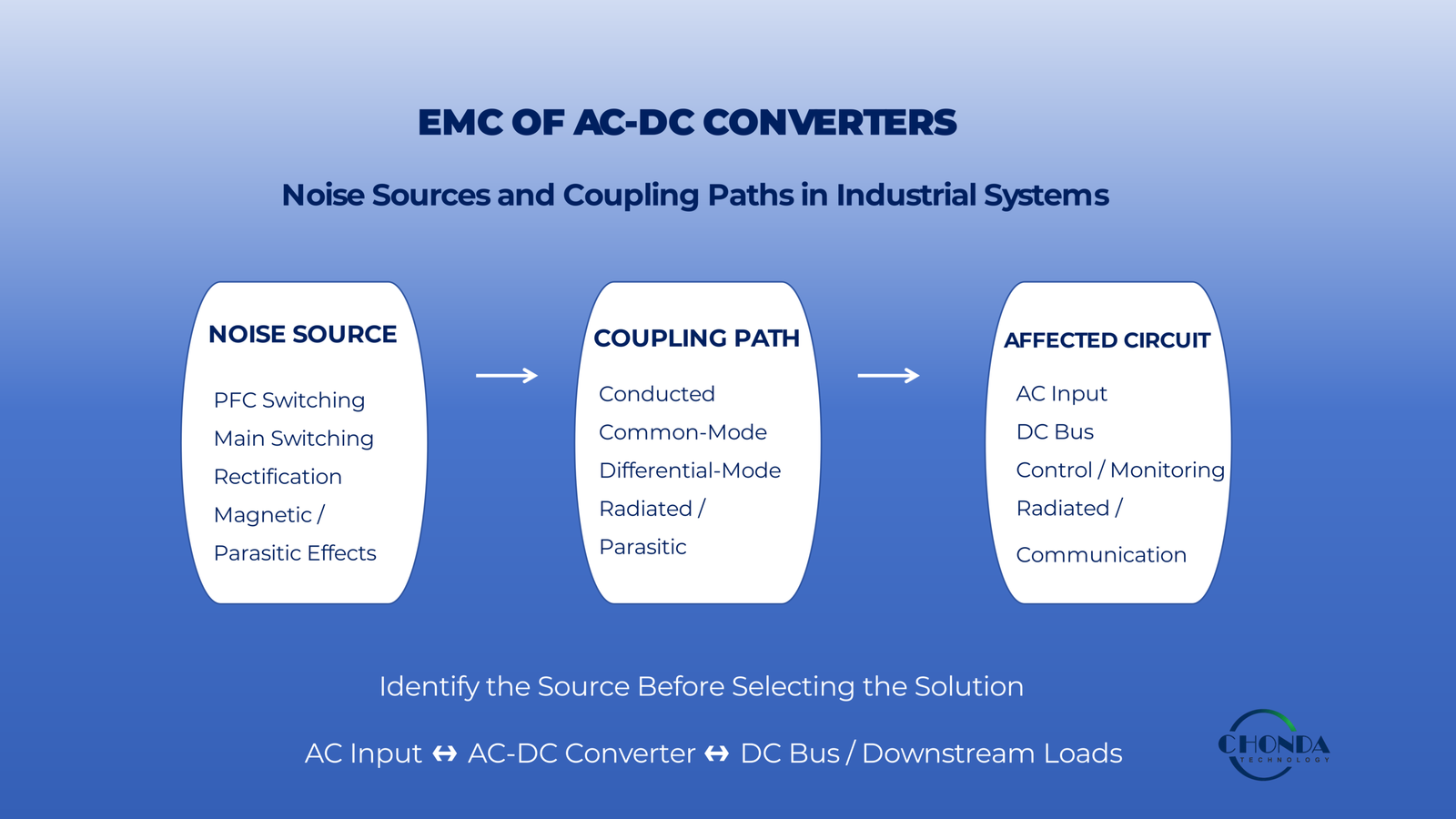
A practical way to understand AC-DC EMC problems is to look at three elements:
Noise Source → Coupling Path → Affected Circuit
The noise source may come from switching transitions, rectification, PFC operation, parasitic capacitance, or rapidly changing input and output currents.
The coupling path may be through:
- Conductors
- Ground or protective earth
- Parasitic capacitance
- Transformer structures
- PCB traces
- The AC input network
- The DC output network
- Radiated electromagnetic fields
The affected circuit may be another power stage, a monitoring circuit, a communication interface, a sensor, or equipment connected to the same AC distribution network.
This means that an EMC problem cannot always be solved simply by adding a larger filter.
The engineer first needs to understand where the noise is generated, how it travels, and where it becomes disruptive.
This is especially important for industrial AC-DC converters because the front end is directly connected to the external AC power network while also supplying the internal DC architecture of the equipment.
The EMC behavior of the converter can therefore influence both sides of the system:
AC Input ↔ AC-DC Converter ↔ DC Bus / Downstream Loads
This guide examines the common EMC noise sources in AC-DC converters and explains how engineers can analyze the noise path, distinguish common-mode and differential-mode problems, evaluate the role of PFC and parasitic coupling, and develop a practical EMC design strategy without treating EMC as a last-minute compliance problem.
1. Where Does EMC Noise Come From in an AC-DC Converter?
The first step in analyzing the EMC performance of an AC-DC converter is to identify where electromagnetic noise is generated.
An AC-DC converter contains several stages that can produce electrical disturbances, but the most important sources are usually associated with rapidly changing voltage and current.
A useful starting point is:
Switching Activity → Noise Source → Coupling Path → Affected Circuit
The noise source may be located in the rectifier, PFC stage, switching stage, magnetic components, or even in the interconnections between these elements.
1.1 Switching Devices
Power semiconductors are often one of the primary sources of high-frequency noise.
During turn-on and turn-off, the voltage and current across a switching device can change rapidly.
These transitions create high dv/dt and di/dt, which can excite parasitic inductance and capacitance within the converter.
The resulting ringing, voltage overshoot, and high-frequency current can then become part of the converter’s electromagnetic environment.
This means that EMC performance is influenced not only by the switching frequency, but also by how fast the switching transitions occur.
1.2 Rectification Stage
The rectifier is another source that should not be overlooked.
In a basic AC-DC front end, the rectifier determines how current is drawn from the AC source and how the rectified waveform feeds the DC-link section.
When the rectifier and bulk capacitor create short input-current pulses, the resulting current waveform contains harmonic components that can propagate toward the AC input.
In more advanced front ends, the rectifier may operate together with an active PFC stage, which changes the current waveform and introduces additional switching activity.
The rectification stage therefore affects both low-frequency input-current behavior and the high-frequency electromagnetic environment.
1.3 PFC Stage
In industrial AC-DC converters, the PFC stage can become an important EMC noise source because it contains another active switching circuit.
The PFC inductor, power switches, diodes or synchronous devices, and associated control circuitry all participate in high-frequency current transitions.
For example:
AC Input → Rectifier → PFC Switching Stage → DC Bus
Each switching transition can generate energy that may couple through the input network, PCB structures, ground, or parasitic capacitances.
PFC therefore creates an important EMC trade-off:
Better Input-Current Control + Additional High-Frequency Switching Activity
The correct design depends on the complete front-end architecture.
1.4 Transformers and Magnetic Components
Magnetic components can also participate in EMC problems.
A transformer does not only transfer energy between windings. Its parasitic capacitance can provide a high-frequency path between electrical domains.
Fast switching voltages can therefore generate common-mode currents through:
- Interwinding capacitance
- Winding-to-core capacitance
- Winding-to-chassis capacitance
- Other stray capacitances
The magnetic component can therefore become part of the noise-coupling path even when its primary function is power conversion.
This is particularly important in isolated AC-DC converters.
1.5 Capacitors and Rapid Current Changes
Capacitors themselves are not necessarily the primary source of switching noise, but their location and parasitic characteristics can strongly influence how high-frequency current flows.
Every real capacitor has parasitic inductance and resistance.
At high frequencies, these parasitic characteristics can determine whether a capacitor effectively provides the intended high-frequency current path.
A capacitor that appears suitable from its nominal capacitance value may therefore behave differently at the switching frequencies of the converter.
This is one reason EMC analysis must consider the physical implementation rather than relying only on schematic values.
1.6 PCB Conductors and Interconnections
High-frequency current does not follow only the ideal schematic.
It also travels through:
- PCB traces
- Copper planes
- Vias
- Connectors
- Wiring
- Mechanical structures
Parasitic inductance in these paths can generate additional voltage disturbances when current changes rapidly.
Likewise, a large current loop can increase the area through which electromagnetic energy can couple into nearby structures.
The physical arrangement of the converter therefore becomes part of its EMC behavior.
Detailed PCB-level mitigation is covered separately in High Voltage DC-DC Converter PCB Design Considerations.
1.7 The DC Bus Can Also Carry High-Frequency Disturbances
The DC bus is not automatically a quiet electrical node simply because it is DC.
Switching currents from downstream or front-end stages can produce ripple and high-frequency disturbances on the bus.
These disturbances may propagate between:
AC-DC Front End ↔ DC Bus ↔ Downstream DC-DC Converters
This is particularly important in multi-stage industrial power systems, where one converter can become the noise source for another.
The DC bus should therefore be considered part of the EMC network rather than simply a power-distribution node.
1.8 Noise Can Be Created by the Interaction of Several Sources
Real EMC problems are often caused by several noise mechanisms acting together.
For example, a PFC stage may create a high-frequency current transition, while a transformer provides a parasitic capacitive path and the PCB provides a low-impedance return route.
The measured EMC problem may therefore appear at the AC input even though the original switching event occurred elsewhere in the converter.
This is why identifying the location of the measured noise does not necessarily identify the original noise source.
1.9 Start With the Source, Not the Filter
When an AC-DC converter fails an EMC test, the first question should not automatically be:
“Which filter should we add?”
A better starting point is:
“What switching event is generating the unwanted energy?”
Then ask:
Where is the energy coupling?
What path is carrying it?
Which circuit is being affected?
This creates a more useful engineering sequence:
Noise Source → Coupling Path → Affected Circuit
Once the main noise sources have been identified, the next step is to understand whether the disturbance is mainly traveling through conductors as conducted noise or coupling through space and parasitic structures as radiated or common-mode noise.
2. How EMC Noise Travels Through an AC-DC Converter
Identifying the noise source is only the first step in AC-DC converter EMC analysis.
The next question is how the unwanted electrical energy travels from the source to the surrounding system.
A useful way to think about an EMC problem is:
Noise Source → Coupling Path → Affected Circuit
The same switching event can create different EMC problems depending on the path available to the high-frequency energy.
In practical AC-DC converters, noise may travel through conductors, parasitic capacitance, grounding structures, magnetic coupling, or free space.
2.1 Conducted Noise
Conducted noise travels through an electrical connection.
In an AC-DC converter, this may include the:
AC Input Path
or:
DC Output / DC Bus Path
For example, switching activity inside a PFC stage may create high-frequency current that travels back toward the AC input through the input wiring and filtering network.
Likewise, switching disturbances can propagate from the AC-DC front end onto the DC bus and reach downstream DC-DC converters.
This is why a converter can create an EMC problem at a point that is physically far away from the original switching device.
The electrical connection itself provides the path.
2.2 Differential-Mode Noise
Differential-mode noise is associated with unwanted voltage or current appearing between two conductors that normally carry the intended power current.
In an AC-DC converter, differential-mode disturbances can be related to:
- Pulsating input current
- Switching current
- Rectifier behavior
- PFC current transitions
- DC-link ripple
A simplified path can be represented as:
Switching Stage → Input Current Disturbance → AC Line Conductors
The important point is that differential-mode noise follows the normal electrical power path.
This makes the current waveform and the impedance of that path important parts of EMC analysis.
2.3 Common-Mode Noise
Common-mode noise follows a different kind of path.
Instead of flowing between the normal power conductors, high-frequency current can flow between the converter and a reference such as protective earth, chassis, or another electrical structure.
A simplified example is:
Switching Node → Parasitic Capacitance → Chassis / Earth → Source
This can happen because real converters contain unavoidable parasitic capacitances.
In an isolated AC-DC converter, for example, high-frequency switching voltage can couple through transformer interwinding capacitance or through capacitance between power structures and the chassis.
The resulting current may then return through a path that was not part of the intended power circuit.
2.4 Why Parasitic Capacitance Matters
At normal power frequency, a parasitic capacitance may appear relatively insignificant.
At high frequency, however, even a small capacitance can provide a meaningful current path when the voltage is changing rapidly.
This is particularly important when a switching node has high dv/dt.
The relationship can be understood conceptually as:
Higher dv/dt + Parasitic Capacitance → Greater High-Frequency Coupling
This is why changing the physical structure of a transformer, heat sink, enclosure, or PCB can sometimes change EMC performance even when the electrical schematic has not changed.
2.5 Radiated Coupling
Not all EMC energy needs a conductive path.
Rapidly changing current loops and switching nodes can also generate electromagnetic fields that couple into nearby circuits or structures.
A simple example is:
High-Frequency Current Loop → Electromagnetic Field → Nearby Circuit
This can become more noticeable when:
- Switching edges are fast
- Current loops are large
- Sensitive circuits are located nearby
- Conductive structures are positioned close to switching nodes
The result may appear as interference in a communication signal, measurement circuit, sensor, or control interface.
2.6 The Same Noise Source Can Use More Than One Path
An important practical point is that one switching event can create several coupling paths at the same time.
For example:
PFC Switching Event
may simultaneously produce:
- Differential-mode current on the AC input
- Common-mode current through parasitic capacitance
- Radiated energy around the switching loop
- High-frequency disturbance on the DC bus
This explains why improving one EMC path does not always eliminate the complete problem.
The noise source may still be coupling through another route.
2.7 The AC Input and DC Bus Are Connected Through the EMC Network
In a two-stage industrial architecture:
AC Input → AC-DC → DC Bus → DC-DC
the AC input and DC bus should not be treated as completely separate EMC environments.
High-frequency energy can move between them through the converter’s internal switching structures and parasitic paths.
For example, noise generated inside the AC-DC front end may appear on the DC bus.
Conversely, a downstream DC-DC converter may inject high-frequency disturbances onto the DC bus that eventually couple back toward the AC input.
The complete power architecture therefore matters when diagnosing EMC behavior.
2.8 Ground and Chassis Can Become Part of the Coupling Path
Industrial equipment often contains:
- Protective earth
- Metal chassis
- Heat sinks
- Mounting structures
- Shielded cables
These structures can provide useful controlled return paths, but they can also become unintended routes for high-frequency currents.
A current that travels through a parasitic capacitance into the chassis may eventually return through protective earth or another connected structure.
The physical installation therefore becomes part of the EMC problem.
2.9 The Location of the Measured Noise Is Not Necessarily the Source
This is an important troubleshooting principle.
Suppose excessive noise is measured at the AC input.
That does not automatically mean the input section itself is generating the noise.
The actual source may be:
PFC Switch → Transformer Parasitic Capacitance → Chassis → AC Input
The measurement location is simply where the unwanted energy becomes visible.
Engineers should therefore trace backward from the measured disturbance to the switching event and coupling path that created it.
2.10 A Practical EMC Path Model
A useful conceptual model for AC-DC converters is:
Noise Source
↓
Conducted / Common-Mode / Radiated Coupling Path
↓
Affected Circuit
↓
Measured EMC Problem
This model helps separate three questions that are often mixed together:
Where is the noise generated?
How is it traveling?
Where does it become a problem?
Only after these questions are understood does it make sense to choose the most appropriate mitigation method.
For detailed EMI filtering, grounding, return-path, and PCB implementation techniques, see High Voltage DC-DC Converter EMI Design Considerations and High Voltage DC-DC Converter PCB Design Considerations.
The practical principle is:
An EMC problem is usually easier to solve when the coupling path is identified before the mitigation method is selected.
3. Common EMC Noise Sources in AC-DC Converter Stages
Once the main coupling paths are understood, engineers can begin to locate the parts of an AC-DC converter that are most likely to generate or amplify EMC problems.
Although the exact noise behavior depends on the topology, the most common problem areas are usually associated with the rectifier, PFC stage, DC-link, switching stage, and magnetic components.
The important point is that these stages do not create noise in exactly the same way.
A useful EMC review therefore asks not only:
Which component is switching?
but also:
What type of electrical transition is occurring, and what coupling path does it create?
3.1 Rectifier and Input-Current Pulses
The rectifier is the first major electrical transition point after the AC input.
In a simple AC-DC front end, a diode bridge combined with a bulk DC-link capacitor can draw current in relatively short intervals near the peaks of the AC waveform.
This creates a highly non-sinusoidal input current.
Although this behavior is primarily associated with power quality and harmonic content, the resulting current pulses also contain higher-frequency components that can interact with the input wiring and filtering network.
The practical implication is that the AC input waveform should be considered part of the EMC behavior of the complete front end.
3.2 PFC Switching Stage
The PFC stage introduces another important source of high-frequency activity.
In an active PFC design, power semiconductor devices switch rapidly while controlling the input current.
This creates changing:
- Voltage
- Current
- dv/dt
- di/dt
These transitions can generate both differential-mode and common-mode disturbances.
The PFC inductor and switching loop are particularly important because the current path changes rapidly during each switching cycle.
A poorly controlled PFC switching environment can therefore create noise that propagates toward both the AC input and the downstream DC bus.
3.3 DC-Link Capacitors and High-Frequency Current Loops
The DC-link capacitor has an important role in the power architecture, but its physical connection also affects EMC behavior.
During switching transitions, high-frequency current may circulate through the local DC-link and switching devices.
The effectiveness of this current path depends on:
- Capacitor placement
- Parasitic inductance
- Connection length
- PCB structure
- Switching frequency
A capacitor that is electrically correct on the schematic may still be ineffective at high frequency if the physical current loop is too large or contains excessive parasitic inductance.
This is one reason EMC performance cannot be predicted from component values alone.
3.4 Main Switching Stage
In an isolated or regulated AC-DC converter, the main switching stage is often one of the strongest sources of high-frequency electromagnetic energy.
The switching devices may generate rapid voltage transitions while transferring energy through a transformer or another magnetic structure.
The resulting noise can then reach:
- Primary-side input circuits
- Secondary-side output circuits
- Chassis
- Protective earth
- Downstream DC-DC converters
The switching node itself may therefore become a major source of common-mode coupling.
3.5 Transformer Parasitic Capacitance
The transformer performs the intended function of power transfer and electrical isolation.
However, the physical structure of the windings also creates unavoidable parasitic capacitance.
When the primary-side voltage changes rapidly, displacement current can flow through these parasitic capacitances toward the secondary side, core, or surrounding structures.
This can create common-mode noise even when there is no intentional conductive connection between the two sides.
The EMC behavior of an isolated AC-DC converter is therefore strongly influenced by transformer construction.
3.6 Heatsinks and Chassis Structures
Metallic structures can become part of an EMC path even when they are not part of the intended power circuit.
A heatsink located near a high-dv/dt switching node may experience capacitive coupling.
The coupled current can then flow through the heatsink, chassis, protective earth, or another connected structure.
This is particularly relevant in industrial equipment where large conductive enclosures and grounded mechanical structures are common.
A mechanically useful structure can therefore become an electrically important structure at high frequency.
3.7 High-Current Interconnections
Input wiring, bus bars, connectors, and PCB copper can also contribute to EMC behavior.
When high-current paths change rapidly, their parasitic inductance can create voltage disturbances.
Longer conductors can increase:
- Loop inductance
- Voltage overshoot
- Ringing
- Unwanted coupling
This does not mean that every high-current connection is automatically an EMC problem.
The issue is whether the physical connection allows significant high-frequency energy to circulate through an uncontrolled path.
3.8 Control and Gate-Drive Circuits
The gate-drive system is another area where EMC behavior can originate.
Fast gate transitions can create high-frequency currents through the gate-drive loop and associated parasitic capacitances.
These signals may couple into:
- Control circuits
- Feedback networks
- Current sensors
- Communication interfaces
A converter can therefore experience control-related EMC problems even when its main power path appears correctly designed.
3.9 DC Output and Downstream Converter Interaction
The AC-DC converter may also become an EMC source for the power stages connected to its DC output.
For example:
AC-DC → DC Bus → DC-DC Converter
The downstream DC-DC converter may contain its own switching activity, creating a combined electromagnetic environment on the common DC bus.
The AC-DC stage and DC-DC stage can therefore interact through:
- Shared input impedance
- DC-bus capacitance
- Common-mode paths
- Return-current structures
An EMC issue observed in the downstream converter does not automatically mean that the downstream converter is the original source.
The front-end and downstream stages should be analyzed together when they share a common power architecture.
3.10 Noise Sources Often Form a Chain
Real EMC failures often result from several interacting mechanisms rather than one defective component.
A typical sequence may be:
PFC Switching → DC-Bus Disturbance → Transformer / Parasitic Coupling → Chassis Current → AC Input or Sensitive Circuit
This illustrates why EMC troubleshooting can be difficult.
The component generating the noise may be physically separated from the location where the problem is measured.
3.11 A Practical Source Review
When reviewing an AC-DC converter for EMC, engineers can begin by identifying:
Where are the fastest voltage transitions?
Where are the highest di/dt current paths?
Which components have significant parasitic capacitance?
Which structures are connected to chassis or protective earth?
Where can high-frequency current circulate?
These questions are often more useful at the beginning of EMC analysis than immediately selecting filters.
The key principle is:
The dominant EMC source is usually associated with a high-frequency electrical transition and the parasitic path that allows its energy to escape the intended power circuit.
Once these common sources have been identified, the next step is to distinguish the main types of AC-DC EMC disturbance and determine whether the problem is primarily differential-mode, common-mode, or a combination of both.
4. Differential-Mode and Common-Mode Noise
Once the main EMC noise sources have been identified, engineers need to understand how the unwanted energy is traveling through the AC-DC converter.
Two important categories are differential-mode noise and common-mode noise.
The distinction is useful because the two types of disturbance follow different electrical paths and often require different design approaches.
A simple way to think about them is:
Differential-Mode → Noise between power conductors
Common-Mode → Noise between the power system and a reference such as chassis or earth
In a real converter, both can occur at the same time.
4.1 Differential-Mode Noise
Differential-mode noise appears between the conductors that normally carry the intended power current.
On the AC input side, this means that unwanted high-frequency current flows between the line conductors.
A simplified path is:
AC Line → Converter → AC Neutral / Return
The disturbance is therefore associated with the normal power circuit.
In an AC-DC converter, differential-mode noise can be influenced by:
- Rectifier current pulses
- PFC switching
- DC-link ripple
- Switching current
- Input impedance
- Wiring inductance
The current waveform generated by the converter is therefore an important part of differential-mode EMC behavior.
4.2 Why Differential-Mode Noise Can Be Easier to Trace
Because differential-mode noise follows an intentional electrical path, it can sometimes be easier to trace through the schematic and current loop.
For example, if a PFC switching stage creates a high-frequency input-current disturbance, the engineer can follow the current path through the input conductors and associated filter components.
The key question is:
Where does the unwanted current flow between the power conductors?
This helps separate a differential-mode problem from a common-mode problem.
4.3 Common-Mode Noise
Common-mode noise follows a different path.
The unwanted high-frequency current may flow from a switching node into the chassis, protective earth, another electrical structure, or another circuit through parasitic capacitance.
A simplified path might be:
Switching Node → Parasitic Capacitance → Chassis / Earth → AC Input
The return path may therefore exist outside the normal power circuit.
This is why common-mode problems can sometimes be difficult to locate from the schematic alone.
4.4 Why Common-Mode Noise Is Important in Isolated AC-DC Converters
Isolation does not automatically eliminate high-frequency coupling.
An isolated AC-DC converter may have no intentional DC connection between primary and secondary, yet high-frequency current can still cross the isolation barrier through parasitic capacitance.
For example, transformer interwinding capacitance can provide a path for displacement current when the primary-side switching voltage changes rapidly.
The result can be:
Primary Switching → Parasitic Capacitance → Secondary / Chassis → Return Path
This is one reason transformer construction can have a significant influence on common-mode EMC behavior.
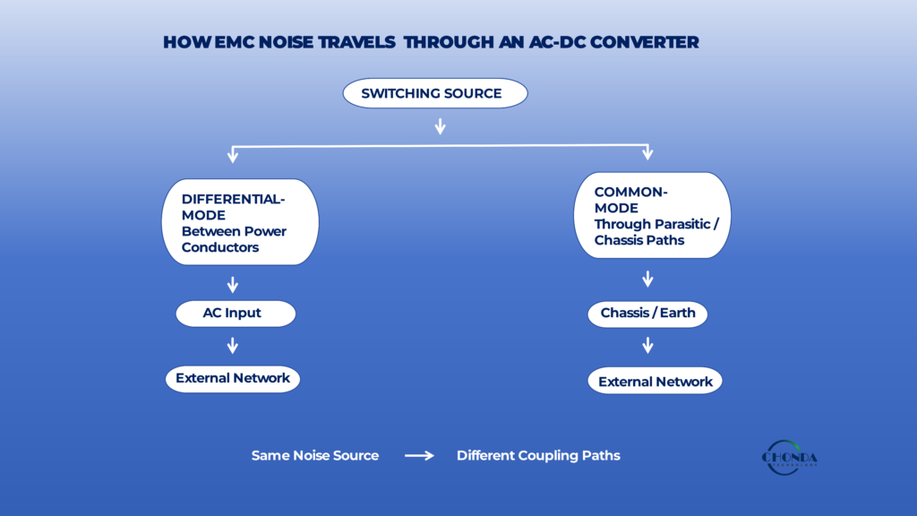
4.5 Differential and Common Mode Can Exist at the Same Time
A single switching event may create both types of disturbance.
For example, a PFC transition may create:
Differential-Mode
High-frequency current between the AC conductors.
At the same time:
Common-Mode
High-frequency current through parasitic capacitance toward chassis or earth.
The measured EMC problem may therefore be a combination of several mechanisms rather than a single clearly separated mode.
4.6 The Physical Structure Can Change the Dominant Mode
The same electrical topology can show different EMC behavior depending on how the components are physically arranged.
For example, changing:
- Transformer construction
- Heatsink position
- PCB geometry
- Chassis connection
- Cable routing
can change the available parasitic paths.
A design that originally had mostly differential-mode noise may therefore develop a stronger common-mode component after a mechanical or layout change.
This is one reason EMC should be evaluated after the converter has been integrated into the actual equipment.
4.7 Common-Mode Noise Can Travel Far from the Source
Because common-mode current can use chassis, earth, cable shields, and other system structures as return paths, the visible problem may appear far away from the original switching device.
For example, a switching event inside the AC-DC converter may eventually cause interference on:
- A communication cable
- A monitoring circuit
- A sensor
- The equipment enclosure
- Another connected power supply
The physical distance between the noise source and the affected circuit does not necessarily indicate that they are electrically unrelated.
The high-frequency return path may connect them.
4.8 The DC Bus Can Carry Both Types of Disturbance
In a two-stage architecture:
AC → AC-DC → DC Bus → DC-DC
the DC bus can become a shared path for high-frequency disturbances.
Differential-mode ripple may appear between the bus conductors.
Common-mode current may couple between the bus and chassis or earth through parasitic capacitances.
This means that an EMC problem measured on the DC side may originate in the AC-DC front end, the downstream DC-DC stage, or their interaction.
4.9 How to Think About the Difference
A practical mental model is:
Differential-Mode
Where is unwanted current flowing between the normal power conductors?
Common-Mode
Where is unwanted current flowing between the power system and another reference such as chassis or earth?
This distinction helps engineers identify the likely coupling path before selecting a mitigation method.
4.10 Do Not Assume the Noise Type from the Measurement Location
A disturbance measured at the AC input is not automatically differential-mode.
Likewise, a disturbance observed near the chassis does not automatically prove that the original source is common-mode.
The measurement point only shows where the unwanted energy has become visible.
The underlying mechanism still needs to be traced back to:
Noise Source → Coupling Path → Affected Circuit
This is especially important when several high-frequency paths exist simultaneously.
4.11 The Practical EMC Principle
For AC-DC converters, differential-mode and common-mode noise should be treated as different manifestations of the same larger problem: unwanted high-frequency energy escaping the intended power-conversion path.
A practical analysis therefore asks:
What is switching?
Which conductors carry the unwanted current?
Can the current return through chassis or earth?
Which parasitic capacitances provide an alternative path?
Where does the disturbance become visible?
Once the dominant noise mode and its coupling path are understood, engineers can make more informed decisions about filtering, grounding, transformer construction, shielding, and physical layout.
5. How PFC and the DC-Link Affect AC-DC EMC
The PFC and DC-link stages play an important role in the EMC behavior of an AC-DC converter because they sit directly between the AC input and the downstream switching stages.
The PFC controls how power is drawn from the AC source, while the DC-link provides the energy-storage interface for the rest of the converter.
Both functions can therefore influence the frequency content, current paths, and coupling mechanisms that determine the converter’s EMC performance.
5.1 PFC Controls the Input Current Waveform
One of the main purposes of an active PFC stage is to shape the input current so that it follows the AC voltage waveform more closely.
From an EMC perspective, this creates two different effects.
At the lower frequency associated with the AC line, better current shaping can reduce unwanted harmonic content.
At the switching frequency and its associated harmonics, however, the PFC stage introduces additional high-frequency switching activity.
The engineer therefore needs to consider both:
Input Current Quality
and:
High-Frequency Switching Noise
A PFC stage that performs well from a power-factor perspective can still require careful EMC design at higher frequencies.
5.2 The PFC Switching Loop Is a Critical Noise Region
The PFC stage normally contains a high-current switching path that changes rapidly during each switching cycle.
This region can generate significant di/dt and dv/dt.
The physical current loop associated with the PFC stage therefore becomes important because unwanted high-frequency energy can couple into nearby structures or return through parasitic paths.
For example:
PFC Switch → Inductor → Rectifier / Capacitor → Return Path
If the high-frequency loop is not well controlled, the switching energy can become more difficult to contain.
This is one reason a converter can show acceptable low-frequency input-current behavior while still experiencing high-frequency conducted or radiated disturbances.
5.3 The DC-Link Connects the Front End to the Switching Stage
The DC-link sits between the front-end rectification/PFC section and the main switching stage.
From a power perspective, it provides energy storage and stabilizes the bus.
From an EMC perspective, it can also become a shared path through which high-frequency energy moves between the two sections.
For example:
PFC → DC-Link → Main Switching Stage
If the DC-link does not provide a sufficiently controlled high-frequency current path, switching disturbances may propagate more widely through the converter.
This means that the DC-link capacitor network should be considered not only for capacitance and ripple-current requirements, but also for its high-frequency behavior.
5.4 Capacitor Parasitics Matter at Switching Frequencies
The nominal capacitance of a DC-link capacitor does not fully describe its behavior at high frequency.
Real capacitors contain parasitic resistance and inductance.
As frequency increases, these parasitic elements become increasingly important and can affect the impedance of the current path.
A capacitor that looks large enough from its rated capacitance may therefore provide a less effective high-frequency path than expected.
The physical connection between the capacitor and switching devices also matters because PCB traces, vias, terminals, and other connections introduce additional parasitic inductance.
5.5 DC-Link Ripple and High-Frequency Noise Are Different Problems
It is useful to distinguish between ordinary DC-link ripple and high-frequency switching noise.
Low-frequency or twice-line-frequency ripple may be primarily related to the AC input and energy-storage requirements.
High-frequency disturbances are more closely associated with switching transitions and parasitic paths.
Both can exist on the same DC bus, but they may require different analysis and design approaches.
This distinction is important because solving a low-frequency ripple problem does not automatically solve a high-frequency EMC problem.
5.6 The PFC and Main Switching Stage Can Interact
In a multi-stage AC-DC converter, the PFC and main switching stage operate from the same internal energy path.
A change in the operating behavior of one stage can therefore affect the electrical environment seen by the other.
For example, the main switching stage may draw pulsed current from the DC-link, creating high-frequency disturbances that propagate back toward the PFC stage.
Likewise, the PFC stage may introduce disturbances onto the bus that become part of the input environment seen by the main switching stage.
The interaction can therefore be viewed as:
AC Input → PFC → DC-Link → Main Switching Stage
rather than as a collection of completely independent blocks.
5.7 PFC Can Influence Both Conducted and Common-Mode Noise
PFC-related noise can appear through more than one coupling path.
The switching current can contribute to differential-mode disturbance on the AC input.
At the same time, rapid switching voltages can drive common-mode current through parasitic capacitances associated with the switch node, heat sink, inductor, chassis, or other structures.
The engineer therefore should not assume that a PFC problem will appear in only one EMC measurement.
Its effects depend on the available coupling paths.
5.8 DC-Link Design Can Affect Downstream EMC
The DC-link is also the interface to any downstream DC-DC stage.
In an architecture such as:
AC → PFC → DC Bus → DC-DC
the DC bus can carry switching disturbances generated by either side.
For example, the downstream DC-DC converter may inject high-frequency current onto the shared bus, while the AC-DC stage provides the return paths through its input and DC-link structures.
This can create an EMC interaction between front-end and downstream stages.
The DC-link should therefore be treated as part of the complete EMC network, not simply as a bulk-energy-storage block.
5.9 The EMC Objective Is to Control High-Frequency Current Loops
A useful engineering perspective is to ask:
Where does the high-frequency current want to flow?
A well-controlled design gives that current a short, predictable, low-impedance path.
A poorly controlled design allows the current to spread into unintended conductors, chassis structures, cables, or parasitic paths.
The PFC and DC-link stages are therefore important because they determine many of the high-frequency current paths between the AC source, switching stage, and DC bus.
5.10 A Practical PFC / DC-Link EMC Review
When reviewing an AC-DC front end, engineers should consider:
PFC Switching Node
→ Where does its high-frequency current return?
DC-Link
→ Does it provide the intended high-frequency current path?
Main Switching Stage
→ How does its current interact with the DC bus?
Parasitic Structures
→ Where can common-mode current escape?
These questions help identify the actual EMC behavior of the front end without reducing the problem to a simple “add more filtering” exercise.
The practical principle is:
PFC and DC-link design influence EMC because they define how high-frequency energy is generated, transferred, and contained between the AC input and the downstream switching stages.
6. How the AC Input and DC Output Can Interact
An AC-DC converter is often treated as having two separate sides: the incoming AC source and the downstream DC bus.
From a power-conversion perspective, this distinction is useful.
From an EMC perspective, however, the two sides are not completely isolated from each other.
High-frequency switching energy generated inside the converter can move between the AC input, the internal DC bus, the primary and secondary structures, and the downstream power system through both intentional electrical connections and parasitic coupling paths.
Understanding this interaction is important when an EMC problem appears on one side of the converter but originates somewhere else.
6.1 The AC Side and DC Side Share the Same Conversion Process
A simplified architecture is:
AC Input → Rectification / PFC → DC Bus → Switching Stage → DC Output
Every stage in this chain is electrically connected to the next one.
A disturbance generated in the PFC stage can therefore propagate toward the DC bus.
A disturbance generated by a downstream switching stage can also appear on the DC bus and influence the front-end input.
The EMC environment of the converter is therefore a network rather than two independent sides.
6.2 Noise Can Travel Through the DC Bus
The DC bus is a common electrical path between different conversion stages.
For example:
AC-DC Front End → DC Bus → DC-DC Converter
If the DC-DC converter produces high-frequency current changes, those currents can create disturbances on the bus.
The disturbance may then couple back into the AC-DC stage or even appear at the AC input through the front-end power path.
This is especially relevant in industrial equipment where several switching converters share the same DC bus.
A measurement showing unwanted noise at the AC input does not therefore prove that the AC input section is the original source.
6.3 Parasitic Capacitance Can Cross the Intended Electrical Boundary
High-frequency current does not need a direct conductive connection to move from one part of the system to another.
Parasitic capacitances can provide alternative paths.
For example:
Primary Switching Node → Transformer Parasitic Capacitance → Secondary Structure
or:
Switching Node → Heat Sink / Chassis Capacitance → Protective Earth
These paths can allow common-mode current to cross boundaries that appear electrically isolated at low frequency.
This is particularly important in isolated AC-DC converters.
6.4 The DC Output Can Carry Noise to Sensitive Electronics
The DC output of an AC-DC converter is intended to provide useful power, but it can also carry unwanted high-frequency disturbances.
These disturbances may reach:
- DC-DC converters
- Control electronics
- Communication circuits
- Sensors
- Measurement systems
For example, an AC-DC front end may meet its nominal output-voltage requirement while still placing high-frequency noise on the DC bus.
A downstream converter may then amplify, redistribute, or couple that energy into a sensitive circuit.
This is one reason output quality should not be judged only by average DC voltage.
6.5 Downstream Converters Can Become Part of the AC-DC EMC Problem
In a multi-stage architecture:
AC Input → AC-DC → DC Bus → DC-DC
the downstream DC-DC converter is part of the same EMC environment.
A DC-DC converter with fast switching transitions can inject high-frequency current onto the shared DC bus.
That current can then interact with the AC-DC front end through:
- DC-bus impedance
- Parasitic capacitance
- Ground structures
- Input filters
- Common-mode paths
This means an EMC problem that appears during system integration may not be visible when either converter is tested independently.
6.6 Input Filters and Output Filters Can Interact
Filters are often designed separately for the AC input and DC output.
However, the complete converter still contains an interconnected energy path.
Changing the impedance of an input or output filter can change the way high-frequency current circulates through the system.
For example, a filter may reduce noise measured at one point while unintentionally redirecting the current through another path.
This is why EMC optimization should consider the complete current loop rather than evaluating each filter in isolation.
6.7 Grounding Can Connect the Two Sides Indirectly
Grounding and chassis structures can create electrical relationships between the AC input and DC output sides even when the intended power path is isolated.
For example, common-mode current may travel:
Switching Node → Parasitic Capacitance → Chassis → Protective Earth → AC Input
The measurement may therefore show noise on the AC side even though the original switching event occurred inside the isolated power-conversion stage.
The ground and chassis system should consequently be treated as part of the EMC architecture.
6.8 Mechanical Changes Can Change Electrical Behavior
The interaction between the AC and DC sides can also change when the physical construction of the converter changes.
For example, moving:
- A heatsink
- A transformer
- A shield
- A cable
- A chassis connection
may change the parasitic capacitance or current-loop geometry.
The schematic may remain exactly the same while the measured EMC performance changes.
This is one of the reasons EMC must ultimately be verified on the actual hardware rather than only from the electrical schematic.
6.9 One Noise Problem Can Appear in Several Measurements
Because multiple paths can exist at the same time, the same underlying switching event may appear as:
- AC input conducted noise
- DC-bus disturbance
- Common-mode current
- Radiated interference
- Communication interference
The measurement location therefore needs to be interpreted together with the suspected coupling path.
A useful troubleshooting sequence is:
Measured Problem → Trace Backward → Identify Coupling Path → Find Original Switching Event
rather than assuming that the component closest to the measurement point is the source.
6.10 Treat the Converter as One EMC Network
The practical way to approach AC-DC EMC is therefore to think of the entire power-conversion system as one connected electromagnetic network:
AC Input ↔ AC-DC Front End ↔ DC Bus ↔ DC-DC / Loads
The boundaries between these sections are useful for architecture, but high-frequency energy can cross them through both conductive and parasitic paths.
The key engineering question is therefore:
Where can high-frequency current travel, and where does that current become a problem?
Once the interactions between the AC side, DC bus, and downstream stages are understood, the next step is to examine how the physical implementation of the converter controls these paths and determines the final EMC behavior.
7. How Physical Design Changes AC-DC EMC Performance
An AC-DC converter can have the same electrical schematic and still produce very different EMC results after the physical design is changed.
This happens because high-frequency currents do not follow an ideal schematic path.
At switching frequencies, PCB traces, component spacing, transformer structures, heat sinks, cables, chassis parts, and even mechanical mounting arrangements become part of the electrical environment.
For this reason, the EMC performance of an AC-DC converter is strongly influenced by where the current flows physically, not only by how the circuit is connected electrically.
7.1 Shorter High-Frequency Paths Usually Provide Better Control
High-frequency current tends to follow the lowest-impedance path available to it.
If the intended switching loop is physically compact, the current can remain concentrated within a controlled region.
If the same loop is spread across a large PCB area, additional parasitic inductance and coupling paths can appear.
For example:
Switch → Inductor / Transformer → Capacitor → Return
should ideally form a controlled high-frequency current path.
A longer physical loop can increase:
- Parasitic inductance
- Voltage overshoot
- Ringing
- Electromagnetic coupling
This is one reason physical placement becomes increasingly important as switching speed increases.
7.2 Component Placement Changes Parasitic Coupling
Two components can be electrically connected correctly while still having an undesirable physical relationship.
For example, placing a high-dv/dt switching node close to:
- A feedback circuit
- A current-sensing trace
- A communication interface
- A sensitive measurement circuit
can increase unwanted capacitive or magnetic coupling.
Moving the sensitive circuit farther away or changing the physical orientation of the power stage can sometimes reduce the disturbance without changing the fundamental circuit topology.
The schematic remains the same.
The electromagnetic environment does not.
7.3 Transformer Placement Can Affect Common-Mode Noise
In an isolated AC-DC converter, the transformer is both a power-transfer component and a potential high-frequency coupling structure.
Its parasitic capacitance can provide a path for common-mode current.
The physical relationship between the transformer, PCB, chassis, heat sink, and surrounding conductors can therefore influence how that current flows.
For example, moving a transformer closer to a chassis structure may change the parasitic capacitance and therefore change the common-mode current path.
The transformer should therefore be considered as part of the EMC architecture rather than as a purely magnetic component.
7.4 Heat Sinks Can Become Electrical Structures
A metal heat sink may exist primarily for thermal reasons, but at high frequency it can also become part of an electromagnetic coupling path.
A switching node located close to a heat sink can capacitively couple high-frequency energy into the metal structure.
That energy may then travel through:
Heat Sink → Chassis → Protective Earth
or another available return path.
This can create common-mode current that eventually appears at the AC input or another connected part of the system.
Thermal and EMC requirements should therefore be considered together when positioning conductive cooling structures.
7.5 Cable Routing Matters
The wiring leaving the converter can become part of the EMC path.
Long AC input cables, DC-bus wiring, output cables, and communication cables can all act as conductors for unwanted high-frequency energy.
The physical relationship between power cables and sensitive signal cables can also influence coupling.
For example, placing a noisy power cable directly alongside a sensitive communication cable for a long distance can increase unwanted coupling even when both circuits are electrically correct.
This is why cable routing should be considered during the mechanical design rather than only after EMC testing.
7.6 Chassis and Grounding Structures Can Redirect Noise
The chassis is often used as part of the EMC control strategy, but it can also become an unintended current path.
A high-frequency current coupled into the chassis may choose a return path that was not anticipated during the schematic design.
For example:
Switching Node → Parasitic Capacitance → Chassis → Cable Shield → External Equipment
This can connect an internal switching event to another part of the installation.
The objective is therefore not simply to connect everything to ground.
It is to provide controlled, predictable high-frequency return paths.
7.7 Layout Changes Can Alter Resonance and Ringing
Parasitic inductance and capacitance can form small resonant networks inside a converter.
The physical dimensions of the circuit determine these parasitic values.
When the layout changes, the resonance frequency and damping can also change.
This can alter:
- Voltage ringing
- Current ringing
- Overshoot
- High-frequency emissions
A layout revision that appears mechanically minor can therefore produce a noticeable change in EMC performance.
7.8 Mechanical Integration Can Affect the EMC Result
The final equipment may contain many structures that were not present in the laboratory prototype.
For example:
- Metal enclosure
- Mounting brackets
- Heat sinks
- Cable trays
- Shields
- External connectors
These structures can change the parasitic environment of the converter.
A prototype that passes an initial EMC test may therefore behave differently after integration into the final enclosure.
This is why EMC validation should ultimately be performed on hardware that is representative of the production configuration.
7.9 Physical Design Should Follow the Noise Path
A useful way to approach the physical design is to start with the expected high-frequency current path.
Ask:
Where does the switching current return?
Where can common-mode current leave the intended circuit?
Which components are exposed to high dv/dt nodes?
Which cables can carry the disturbance outside the enclosure?
These questions help determine where the physical structure needs to be controlled most carefully.
7.10 EMC and PCB Design Are Closely Connected, but Not Identical
PCB layout is an important part of EMC design, but EMC performance is not determined by the PCB alone.
The complete physical environment includes:
PCB + Transformer + Heat Sink + Cables + Chassis + Enclosure + Grounding
All of these structures can influence the high-frequency current paths.
For detailed PCB-level techniques such as loop-area control, return-path design, creepage, clearance, and grounding structures, see High Voltage DC-DC Converter PCB Design Considerations.
The practical principle is:
At high frequency, the physical implementation becomes part of the circuit.
A well-designed AC-DC converter therefore needs both an appropriate electrical topology and a physical structure that keeps high-frequency energy on controlled, predictable paths.
8. EMC Should Be Considered from the Beginning
EMC problems are often more difficult and expensive to solve when they are discovered only after the first complete prototype has been built.
At that stage, the converter architecture, PCB layout, transformer construction, enclosure, cooling structure, and cable routing may already be fixed.
A late EMC problem can then require changes across several parts of the system.
For this reason, EMC should be considered from the beginning of AC-DC converter development rather than treated as a final compliance step.
8.1 Start With the Power Architecture
The first EMC decisions are often made before the PCB is designed.
The system architecture determines:
- Where the AC input enters
- Where the PFC stage is located
- Where the DC bus is formed
- Where isolation occurs
- Which circuits share a power domain
- Where sensitive loads are connected
These decisions influence the possible noise paths throughout the converter.
For example, placing a sensitive monitoring circuit directly next to a high-dv/dt switching stage can create a difficult coupling problem that would have been easier to avoid at the architecture stage.
8.2 Identify High-Noise Regions Early
Engineers can identify likely high-noise regions before detailed hardware is complete.
Typical candidates include:
- PFC switching nodes
- Main switching devices
- Transformer primary structures
- High-current commutation loops
- Fast gate-drive circuits
- DC-link switching paths
These regions can then be treated as controlled electromagnetic zones during the physical design.
The objective is not to eliminate switching activity.
It is to prevent high-frequency energy from spreading into unintended paths.
8.3 Define the Important Return Paths
One of the most useful early EMC questions is:
Where will the high-frequency current return?
The intended return path should be defined as part of the power-stage design.
If the return path is left to whatever conductors, chassis structures, or parasitic capacitances happen to be available, the converter may develop unexpected common-mode currents and ringing.
Controlled return paths are therefore one of the foundations of predictable EMC behavior.
8.4 Consider the Filter and Converter Together
Input and output filtering should also be considered as part of the converter architecture.
A filter is not simply a box placed between the converter and the external system.
Its impedance interacts with the power stage and can influence:
- Current ripple
- Resonance
- Startup behavior
- Control response
- High-frequency current paths
The filter should therefore be developed together with the converter rather than added only after an EMC failure.
8.5 Use Simulation and Early Measurements
Simulation can help engineers identify possible resonances, switching overshoot, and current paths before the final hardware is available.
However, simulation does not replace measurement.
Even a detailed model may not fully represent:
- Transformer parasitic capacitance
- Mechanical structures
- Connector geometry
- Chassis coupling
- Cable routing
- Manufacturing variation
Early prototype measurements can therefore reveal unexpected EMC behavior before the design becomes difficult to change.
8.6 Test Under Representative System Conditions
EMC performance can change when the converter is connected to its final environment.
The test setup should therefore approximate the real equipment as closely as practical.
Relevant conditions may include:
- Minimum and maximum input voltage
- Typical and maximum load
- Different operating modes
- Connected DC-DC converters
- Final enclosure
- Actual cables
- Protective earth connections
- Representative grounding
A converter that passes a simplified bench test may still behave differently after complete system integration.
8.7 Fix the Source Before Adding More Filtering
When an EMC measurement exceeds the target, the easiest reaction may be to add another filter or increase an existing filter.
Sometimes that is effective.
However, if the root cause is excessive switching overshoot, an uncontrolled current loop, or an unintended common-mode path, additional filtering may only mask the symptom or move the problem elsewhere.
A more systematic approach is:
Identify the Noise Source
↓
Identify the Coupling Path
↓
Reduce the Source or Control the Path
↓
Then Optimize the Filter
This approach often leads to a more robust design.
8.8 EMC Changes Can Affect Other Design Targets
An EMC modification should also be checked against the rest of the converter.
For example:
- Increasing filtering may increase losses.
- Adding a common-mode path may increase leakage current.
- Changing switching speed may affect efficiency.
- Changing transformer construction may affect insulation.
- Increasing physical spacing may affect power density.
- Adding shielding may affect thermal performance.
The best EMC solution is therefore rarely the one that optimizes EMC alone.
It is the one that improves electromagnetic compatibility while preserving the required electrical, thermal, safety, and mechanical performance.
8.9 Build EMC Into the Development Sequence
A practical development sequence can be:
Architecture
↓
Identify Noise Sources
↓
Define Coupling Paths
↓
Physical Design
↓
Prototype Measurement
↓
Targeted EMC Improvement
↓
System Validation
This makes EMC part of the design process rather than an isolated certification activity near the end of development.
8.10 The Practical Principle
The most useful mindset is:
EMC should be designed into the converter, not added to the converter.
For AC-DC converters, this means considering the noise source, return path, parasitic coupling, input network, DC bus, chassis, and downstream power architecture from the beginning.
When these relationships are understood early, EMC optimization becomes a controlled engineering process rather than a repeated cycle of failed testing and increasingly complex filters.
9. Practical EMC Design Considerations for AC-DC Converters
Once the major noise sources and coupling paths have been identified, the next step is to decide how the AC-DC converter should be designed to control those disturbances.
There is no single EMC component or circuit that solves every problem.
A practical design usually combines several decisions around the power stage, physical structure, current paths, filtering, grounding, and switching behavior.
The most effective approach is to address the dominant noise mechanism first and then use filtering or shielding as part of the overall strategy.
9.1 Control the Noise Source First
The most effective EMC improvement is often to reduce the unwanted energy at the source.
For example, excessive ringing at a switching node may indicate uncontrolled parasitic inductance or capacitance.
Possible design actions may include:
- Optimizing the switching loop
- Controlling switching speed
- Reducing voltage overshoot
- Improving device selection
- Optimizing gate-drive behavior
- Managing parasitic elements
Reducing the disturbance at its source can improve several EMC paths at the same time.
This is generally more robust than allowing a large amount of high-frequency energy to escape and attempting to remove it later.
9.2 Keep High-Frequency Current Paths Controlled
Once a switching event occurs, the next priority is to provide a predictable return path.
The high-frequency current should remain within a compact, controlled loop whenever practical.
This reduces unwanted coupling into:
- Nearby circuits
- Chassis
- Cables
- Ground structures
- Sensitive signal paths
The exact PCB techniques depend on the topology and implementation and are covered in greater detail in the relevant PCB design guidance.
The architectural principle, however, is simple:
Give high-frequency current a deliberate path instead of allowing it to find one through parasitic structures.
9.3 Use Filtering as Part of the System, Not as a Patch
Input and output filters can reduce conducted disturbances, but they should be designed together with the converter.
An input filter can help prevent high-frequency noise from reaching the AC source.
An output or DC-bus filter can help prevent switching disturbances from propagating toward downstream circuits.
However, every filter introduces its own impedance, losses, physical size, and potential resonance.
The filter therefore needs to be evaluated together with the converter operating conditions.
9.4 Consider Common-Mode Paths Carefully
If the dominant problem is common-mode noise, simply increasing differential-mode filtering may produce little improvement.
Instead, the engineer should examine the available common-mode return path.
For example:
Switching Node → Parasitic Capacitance → Heat Sink / Chassis → Protective Earth
The solution may involve controlling:
- Parasitic capacitance
- Transformer construction
- Shielding
- Chassis connections
- Return-current paths
- Physical spacing
The correct intervention depends on where the common-mode current is actually flowing.
9.5 Control Switching Speed as a Design Variable
Fast switching transitions can reduce certain switching losses, but they can also increase dv/dt, di/dt, ringing, and electromagnetic coupling.
It may therefore be useful to treat switching speed as an optimization variable rather than maximizing it automatically.
For example:
Faster Edge
→ Potentially Lower Switching Time
but also:
→ Higher dv/dt
→ Higher di/dt
→ Greater Parasitic Excitation
The appropriate switching behavior depends on the semiconductor technology, topology, power level, efficiency target, and EMC requirements.
9.6 Pay Attention to the AC Input Network
Because the AC-DC converter is connected directly to the external electrical supply, the input network deserves special attention.
The engineer may need to consider:
- Input filter structure
- Protective earth
- Cable routing
- Connector arrangement
- Surge protection
- Differential-mode current
- Common-mode current
The objective is to control unwanted current before it leaves the equipment and interacts with the external power network.
9.7 Protect Sensitive Circuits from the Noise Source
Not every EMC problem should be solved at the power stage.
Sometimes it is easier and more effective to protect a sensitive circuit from the noise environment.
For example, a monitoring or communication circuit can be separated physically or electrically from a high-dv/dt switching region.
This can involve:
- Physical separation
- Controlled reference structures
- Shielding
- Isolated power
- Filtering at the sensitive interface
The best design often uses both sides of the problem:
Reduce Noise at the Source + Reduce Sensitivity at the Receiver
9.8 Consider EMC and Thermal Design Together
EMC improvements can interact with thermal and mechanical design.
For example, a larger heat sink may provide better thermal performance but also increase parasitic coupling to a switching node.
A shield may reduce electromagnetic coupling while changing airflow.
Additional filtering may reduce noise but introduce more power loss.
These interactions should be checked before finalizing the design.
9.9 Validate Under the Worst Relevant Conditions
EMC performance can change with:
- Input voltage
- Load level
- Switching frequency
- Operating temperature
- Connected downstream converters
- Enclosure configuration
The converter should therefore be tested under the operating conditions that are most likely to create the dominant noise mechanism.
A convenient nominal operating point is not always the worst EMC condition.
9.10 Use a Source-Path-Receiver Strategy
A practical EMC review can be organized around three questions:
Source
What is generating the unwanted high-frequency energy?
Path
How is that energy reaching another circuit or the external environment?
Receiver
Where is the disturbance becoming unacceptable?
This leads to three corresponding design actions:
Reduce the Source
Control the Path
Protect the Receiver
This framework is often more useful than starting with a list of filters or EMC components because it helps engineers choose the intervention that addresses the actual mechanism.
9.11 EMC Is a System Optimization Problem
A robust AC-DC EMC design normally balances:
EMC Performance + Efficiency + Thermal Performance + Safety + Power Density + Cost
Optimizing one parameter in isolation can create a new problem elsewhere.
For example, reducing switching speed may improve EMC but increase switching losses.
Increasing filtering may reduce conducted noise but increase size and loss.
Increasing isolation structures may improve safety while making thermal management more difficult.
The objective is therefore to find a practical operating and physical design point in which the complete converter satisfies its electrical and system requirements.
9.12 The Practical EMC Principle
A high-quality AC-DC EMC design can be summarized as:
Identify the Source → Control the Coupling Path → Protect Sensitive Circuits → Validate the Complete System
The purpose of EMC design is not simply to make a converter pass one laboratory measurement.
It is to ensure that the converter can operate reliably within its intended industrial environment while remaining compatible with the other electrical and electronic systems around it.
10. EMC Validation in Real Industrial Conditions
An AC-DC converter can perform well during development testing and still show different EMC behavior after it is installed in the final industrial system.
The reason is simple: the electromagnetic environment of the real equipment is usually more complicated than the laboratory setup.
The final enclosure, cable routing, grounding structure, downstream converters, protective earth connections, and nearby switching equipment can all change the available coupling paths.
For this reason, EMC validation should be performed under conditions that represent the actual operating environment as closely as practical.
10.1 Test More Than One Operating Point
EMC behavior can change with operating conditions.
For example, the dominant noise source at light load may not be the same as the one at high load.
Likewise, different AC input voltages can change:
- PFC operating conditions
- Input current
- Switching behavior
- DC-bus voltage
- Power loss
A useful validation process should therefore include representative combinations of:
Minimum Input → Nominal Input → Maximum Input
and:
Low Load → Typical Load → High Load
The exact test points should be determined by the application and applicable requirements.
10.2 Evaluate the Complete Power Architecture
A front-end AC-DC converter should not always be tested completely by itself.
If the final equipment includes:
AC Input → AC-DC → DC Bus → DC-DC → Loads
then the interaction between these stages can become part of the EMC behavior.
A downstream DC-DC converter can introduce additional switching currents onto the DC bus.
Sensitive monitoring or communication circuits can also reveal disturbances that are not visible during isolated converter testing.
The final EMC assessment should therefore include the relevant downstream power architecture whenever practical.
10.3 Use the Final Mechanical Configuration
EMC performance can change when the converter is installed in the actual enclosure.
Metal panels, heat sinks, cable trays, mounting brackets, shields, and connectors can all influence parasitic coupling and current return paths.
For example, moving a heat sink closer to a switching node may change common-mode coupling.
Similarly, changing the routing of a long DC cable may alter the amount of radiated or conducted disturbance reaching another circuit.
The final validation should therefore use a mechanical configuration that is representative of the production equipment.
10.4 Pay Attention to Cable and Grounding Conditions
Cables can become part of the EMC path.
The validation setup should therefore consider the actual:
- AC input cables
- DC output cables
- Communication cables
- Protective-earth connections
- Shielding structures
Changing cable length or grounding can sometimes change the measured result significantly.
This is particularly important in industrial installations where the converter may be connected to long power or communication cables.
10.5 Test the Conditions That Stress the Noise Mechanism
Instead of testing only a convenient nominal operating point, engineers should identify the conditions most likely to increase the dominant noise source.
For example:
High dv/dt Problem
→ Evaluate the relevant switching conditions and operating points.
PFC Input-Current Problem
→ Evaluate different line-voltage and load combinations.
Common-Mode Problem
→ Evaluate the actual chassis, earth, isolation, and cable configuration.
This approach makes EMC testing more diagnostic rather than simply a pass/fail exercise.
10.6 Separate Source Investigation from Compliance Testing
Formal EMC testing determines whether the equipment meets the required limits.
Engineering investigation has a different purpose.
It tries to answer:
Why is the measured noise at this level?
When a result is outside the expected range, engineers can return to the source-path model:
Noise Source → Coupling Path → Affected Circuit
This helps identify whether the issue is related to:
- Switching behavior
- PFC
- Transformer parasitics
- DC-bus interaction
- Grounding
- Cable coupling
- Physical layout
The diagnostic process is often much faster when the measurement is interpreted through the underlying noise mechanism.
10.7 Repeat Tests After Major Design Changes
EMC improvements can affect other parts of the converter.
For example:
- A new filter can change current paths.
- A switching-speed change can alter efficiency and ringing.
- A transformer modification can change common-mode coupling.
- A chassis change can create a different return path.
A design change that improves one measurement should therefore be followed by a broader verification rather than assuming that the EMC problem has been permanently solved.
10.8 Validation Should Represent Real Use
The most useful EMC validation answers one final question:
Will the converter remain electromagnetically compatible when it is operating in the equipment and environment for which it was designed?
That requires more than a single laboratory test.
It requires a representative combination of:
Electrical Conditions + Load Conditions + Mechanical Configuration + Grounding + Cabling + Downstream Power Architecture
The closer the validation environment is to the final installation, the more confidence engineers can have that an EMC improvement will remain effective in production.
10.9 EMC Validation Is the Final Check of the Design Method
A strong EMC design process can therefore be summarized as:
Identify Noise Sources
↓
Understand Coupling Paths
↓
Control Physical and Electrical Paths
↓
Validate Under Representative Conditions
↓
Investigate Any Remaining Problem
The purpose of validation is not simply to obtain a certification result.
It is to confirm that the converter’s noise behavior is consistent with the assumptions made during architecture, circuit, and physical design.
The practical principle is:
The most reliable EMC result is one that has been engineered into the converter and then confirmed under the real conditions in which the equipment will operate.
Conclusion
EMC performance is an important part of AC-DC converter design because the converter operates at the boundary between the external AC power system and the internal DC power architecture.
An effective EMC design process should begin by understanding:
Noise Source → Coupling Path → Affected Circuit
From there, engineers can evaluate the major sources of disturbance, including rectification, PFC switching, DC-link behavior, main switching stages, magnetic components, parasitic capacitance, and physical structures such as heat sinks, cables, and chassis.
The distinction between differential-mode and common-mode noise can then help identify how unwanted high-frequency energy is moving through the system.
For industrial AC-DC converters, EMC performance should also be evaluated across the complete architecture:
AC Input → AC-DC Front End → DC Bus → DC-DC Conversion → Loads
This is important because a noise problem observed at one location may originate elsewhere in the power system.
The most reliable approach is therefore not to treat EMC as a final filtering exercise.
Instead, engineers should control the noise source, provide predictable current-return paths, manage parasitic coupling, protect sensitive circuits, and validate the complete design under representative operating and installation conditions.
The goal is not simply to make an AC-DC converter pass a laboratory test.
It is to create a converter that can operate reliably and compatibly within the real industrial electrical environment for which it was designed.
How CHONDA Approaches EMC in Industrial Power Systems
For CHONDA AC-DC and DC-DC power-module applications, EMC considerations are evaluated together with the electrical architecture, switching behavior, isolation, thermal conditions, mechanical integration, and actual installation environment.
Depending on the application, the appropriate solution may involve standard power modules, modified platforms, or customized power-conversion designs.
For systems with demanding high-voltage input conditions, sensitive monitoring or communication electronics, or unusual mechanical and grounding requirements, EMC should be considered as part of the power architecture from the beginning rather than added after the converter has been completed.
Related Articles
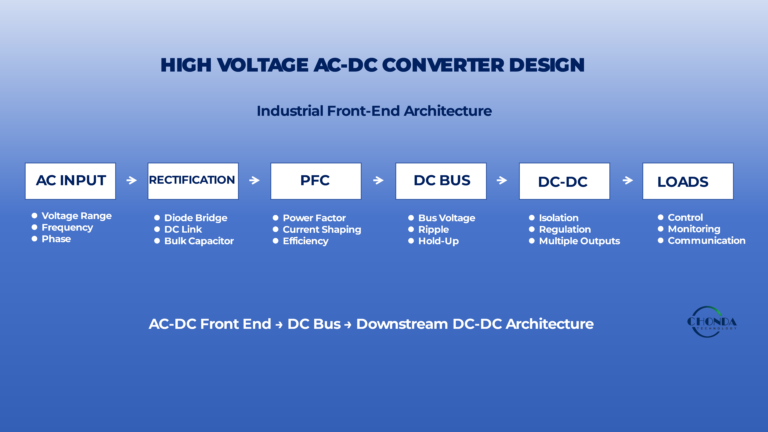
High Voltage AC-DC Converter Design for Industrial Systems
Explore AC-DC front-end design considerations including rectification, PFC, DC-bus formation, isolation, protection, thermal performance, and downstream DC-DC conversion.
High Voltage DC-DC Converter EMI Design Considerations
Explore EMI sources, common-mode and differential-mode noise, filtering, grounding, and electromagnetic considerations for high-voltage DC-DC converters.
High Voltage DC-DC Converter PCB Design Considerations
Understand how PCB layout, switching loops, return paths, creepage, clearance, and physical implementation affect converter performance.
High Voltage Power Supply Design Guide
Review a system-level framework for high-voltage power architecture, including conversion stages, isolation, regulation, thermal management, EMI, protection, and power-module selection.
High Frequency DC-DC Converter Design: Efficiency & EMI
Learn how switching frequency affects magnetic design, switching losses, thermal density, EMI, and power density.
Choosing Between AC-DC and DC-DC Power Modules
Understand the architectural differences between AC-DC and DC-DC conversion and when each approach is appropriate for industrial power systems.